Product Classification
Contact Us
FEEDBACK

Great quality and amazing service. Very fast...

Two days ago to do the board, the quality is quite good, delivery speed, good quality, no reason to not choose here ah.
P*****n 2017-12-14
The board is very fine, the product packaging is also very good, each is an independent packaging, customer service attitude is also very good, very thoughtful service, website pricing system is also very easy to use, very user-friendly design, delivery speed Very fast, very satisfied.
K****n 2017-12-14
This is the use of proofing materials are made of FR-4, a look that is a good plate, the manufacturer's production process is not to say, done very well, the speed is very fast, on-time delivery, online pricing The system is also very easy to use, you can calculate the price directly to complete the funding orders
S*****c 2017-12-14Full Feature PCB Manufacturing
multitech-pcb.com is a professional quick turn PCB prototyping and low-volume production manufacturer located in Shenzhen China. Currently we only accept 4 PCB files format( gerber file, .pcb, .pcbdoc or .cam file format) for PCB fabrication.
In order for us to keep our products and services competitive, we constantly are updating our equipments to better serve our customers. Please send email to sales@multitech-pcb.com if your boards are beyond the capabilities listed below.
Click above to order your PCB prototype or low-volume orders online, and you will be asked to upload your PCB files in ( gerber file, .pcb, .pcbdoc or .cam file format) before check out.
Multitech PCB Capabilities
| Feature | Capability |
| Quality Grade | Standard IPC 2 |
| Number of Layers | 1 - 60 layers |
| Order Quantity | 1pc - 10,000,000 pcs |
| Build Time | 2days - 5weeks (Expedited Service) |
| Material | FR-4 Standard Tg 150°C, FR4-High Tg 170°C, FR4-High-Tg 180°C, FR4-Halogen-free, FR4-Halogen-free & High-Tg,Rogers, Arlon Taconic Nelco |
| Board Size | Min 6*6mm | Max 1200*700mm |
| Board size tolerance | ±0.1mm - ±0.2mm |
| Board Thickness | 0.2mm - 8.0mm |
| Board Thickness Tolerance | ±0.1mm - ±10% |
| Copper Weight | 0.5oz - 12.0oz |
| Inner Layer Copper Weight | 0.5oz - 6.0oz |
| Copper Thickness Tolerance | +0μm +20μm |
| Min Tracing/Spacing | 2mil/2mil |
| Solder Mask Sides | As per the file |
| Solder Mask Color | Green, White, Blue, Black, Red, Yellow, Purple, Grey |
| Silkscreen Sides | As per the file |
| Silkscreen Color | White, Blue, Black, Red, Yellow |
| Surface Finish |
HASL - Hot Air Solder Leveling Lead Free HASL - RoHS ENIG - Electroless Nickle/Immersion Gold - RoHS ENEPIG - Electroless Nickel Electroless Palladium Immersion Gold - RoHS Immersion Silver - RoHS Immersion Tin - RoHS OSP -Organic Solderability Preservatives - RoHS |
| Min Annular Ring | 3mil |
| Min Drilling Hole Diameter | 6mil, 4mil-laser drill |
| Min Width of Cutout (NPTH) | 0.8mm |
| NPTH Hole Size Tolerance | ±.002" (±0.05mm) |
| Min Width of Slot Hole (PTH) | 0.6mm |
| PTH Hole Size Tolerance | ±.003" (±0.08mm) - ±4mil |
| Surface/Hole Plating Thickness | 20μm - 30μm |
| SM Tolerance (LPI) | .003" (0.075mm) |
| Aspect Ratio | 1:40 (hole size: board thickness) |
| Test | 10V - 250V, flying probe or testing fixture |
| Impedance tolerance | ±5% - ±10% |
| SMD Pitch | 0.2mm(8mil) |
| BGA Pitch | 0.2mm(8mil) |
| Chamfer of Gold Fingers | 20, 30, 45, 60 |
| Other Techniques |
Gold fingers Blind and Buried Holes peelable solder mask Edge plating Carbon Mask Kapton tape Countersink/counterbore hole Half-cut/Castellated hole Press fit hole Via tented/covered with resin Via plugged/filled with resin Via in pad Electrical Test |
FLEX PCB
| Feature | Capability |
| Quality Grade | Standard IPC 2 |
| Number of Layers | 1 - 16 layers |
| Build Time | 2days - 5weeks |
| Material | DuPont PI, Domestic Shengyi PI |
| Board Size | 490*1800mm,240*4000mm |
| Board Thickness | 0.04-2.5mm |
| Copper Weight (Finished) | 1/3oz-2oz,6oz |
| Min Tracing/Spacing | 0.035/0.035mm |
| Solder Mask Sides | As per the file |
| Solder Mask Color | Green, White, Blue, Black, Red, Yellow |
| Solder-stop coating---Soldermask oil | Green, White, Blue, Black, Red, Yellow |
| Solder-stop coating---Coverlay | PI and PET film |
| Silkscreen Sides | As per the file |
| Silkscreen Color | White, Black, Yellow |
| Surface Finish |
HASL - Hot air solder leveling Lead - free HASL - RoHS ENIG - RoHS Immersion Tin - RoHS OSP - RoHS |
| Min Annular Ring | |
| Min Drilling Hole Diameter | |
| Min. hole size---Drilling (PTH) | 0.2mil |
| Min. hole size---Punching (NPTH) | 0.05/±0.02mm |
| Tolerance of dimension | ±0.03mm |
| Other Techniques |
Peelable solder mask Gold fingers Stiffener (only for PI/FR4 substrate) |
FLEX, RIGID-FLEX, and HDI SUBSTRATES
| Product | Standard Flex Circuits | Standard Rigid-flex Circuits | High Density Interconnect (HDI) Flex Circuits |
|---|---|---|---|
| Standard Panel Size | 490*1800mm,240*4000mm | 100mm x 100mm | 250mm x 400mm |
| Line Width and Spacing | .001" (0.035mm) | .003" (0.07mm) | .003" (0.07mm) |
| Copper Thickness | 1/3 oz - 2 oz, 6 oz | 1/4 to 1/2 oz. | 1/2 oz. and higher |
| Layer Count | 1-16L | Up to 36L | Up to 18 |
| Surface Finish |
HASL - Hot air solder leveling Lead - free HASL - RoHS ENIG - RoHS Immersion Tin - RoHS OSP - RoHS |
HASL - Hot air solder leveling Lead - free HASL - RoHS ENIG - RoHS Immersion Tin - RoHS OSP - RoHS |
HASL - Hot air solder leveling Lead - free HASL - RoHS ENIG - RoHS Immersion Tin - RoHS OSP - RoHS |
| Via/ Drill Size | |||
| Minimum Drill (Mechanical) Hole Diameter | .008" (0.2 mm) | .006" (0.15 mm) | .008" (0.2 mm) |
| Minimum Via (Laser) Size | 5 mil (0.15 mm) | 1 mil (0.025 mm) | 6 mil (0.15 mm) |
| Minimum Micro Via (Laser) Size | 2 mil (0.05 mm) | 1 mil (0.025 mm) | 3 mil (0.07 mm) |
| Stiffener Material | Polyimide / FR4 / Metal | Polyimide / FR4 / Metal | Polyimide / FR4 |
| Shielding Material | Copper / Silver Ink / Tatsuta / Carbon | Copper / Silver Ink / Tatsuta / Carbon | Copper / Silver Ink / Tatsuta / Carbon |
| Tooling Tolerance | 2 mil (0.05 mm) | 1 mil (0.025 mm) | 2 mil (0.05 mm) |
| Zif Tolerance | 2 mil (0.05 mm) | 1 mil (0.025 mm) | 2 mil (0.05 mm) |
| Solder Mask | |||
| Solder Mask Bridge Between Dam | 5 mil (0.13 mm) | 4 mil (0.11 mm) | 5 mil (0.13 mm) |
| Solder Mask Registration Tolerance | 4 mil (0.11 mm) | 4 mil (0.11 mm) | 5 mil (0.13 mm) |
| Coverlay | |||
| Coverlay Registration | 8 mil (0.20 mm) | 5 mil (0.13 mm) | 8 mil (0.20 mm) |
| PIC Registration | 7 mil (0.18 mm) | 4 mil (0.11 mm) | 7 mil (0.18 mm) |
| Solder Mask Registration | 5 mil (0.13 mm) | 4 mil (0.11 mm) | 5 mil (0.13 mm) |
| Stiffener | |||
| PI Stiffener | |||
| Stiffener Registration | 10 mil (0.25 mm) | 10 mil (0.25 mm) | 10 mil (0.25 mm) |
| Thickness Tolerance | 10% | 10% | 10% |
| FR4 Stiffener | |||
| Stiffener Registration | 10 mil (0.25 mm) | 10 mil (0.25 mm) | Layer to Layer |
| Thickness Registration | 10% | 10% | 5 mil (0.13 mm) |
| Legend | |||
| Minimum Height | 35 mil (0.89 mm) | 25 mil (0.64 mm) | 35 mil (0.89 mm) |
| Minimum Width | 8 mil (0.20 mm) | 6 mil (0.15 mm) | 8 mil (0.20 mm) |
| Minimum Space | 8 mil (0.20 mm) | 6 mil (0.15 mm) | 8 mil (0.20 mm) |
| Registration | +/- 5 mil (0.13 mm) | +/- 5 mil (0.13 mm) | +/- 5 mil (0.13 mm) |
| Impedance | +/- 10% | +/- 10% | +/- 10% |
| SRD (Steel Rule Die) | |||
| Outline Tolerance | 5 mil (0.13 mm) | 2 mil (0.051 mm) | 5 mil (0.13 mm) |
| Minimum Radius | 5 mil (0.13 mm) | 4 mil (0.11 mm) | 5 mil (0.13 mm) |
| Inside Radius | 20 mil (0.51 mm) | 10 mil (0.25 mm) | 31 mil (0.79 mm) |
| Punch Minimum Hole Size | 40 mil (1.02 mm) | 31.5 mil (0.80 mm) | N/A |
| Tolerance of Punch Hole Size | +/- 2 mil (0.051 mm) | +/- 1 mil (0.025 mm) | N/A |
| Slot Width | 20 mil (0.51 mm) | 15 mil (0.38 mm) | 31 mil (0.79 mm) |
| Tolerance of Hole to Outline | +/- 3 mil (0.07 mm) | +/- 2 mil (0.051 mm) | +/- 4 mil (0.11 mm) |
| Tolerance of Hole Edge to Outline | +/- 4 mil (0.11 mm) | +/- 3 mil (0.07 mm) | +/- 5 mil (0.13 mm) |
| Minimum of Trace to Outline | 8 mil (0.20 mm) | 5 mil (0.13 mm) | 10 mil (0.25 mm) |
Upload PCB files( gerber file, .pcb, .pcbdoc or .cam file format)
Thanks for reviewing our PCB capabilities. Please upload your PCB files in the format of gerber file, .pcb, .pcbdoc or .cam file when you go through our online purchase procedures. You can also send your Gerber via email (service@pcbway.com), but we strongly suggest you order online on the webpages.
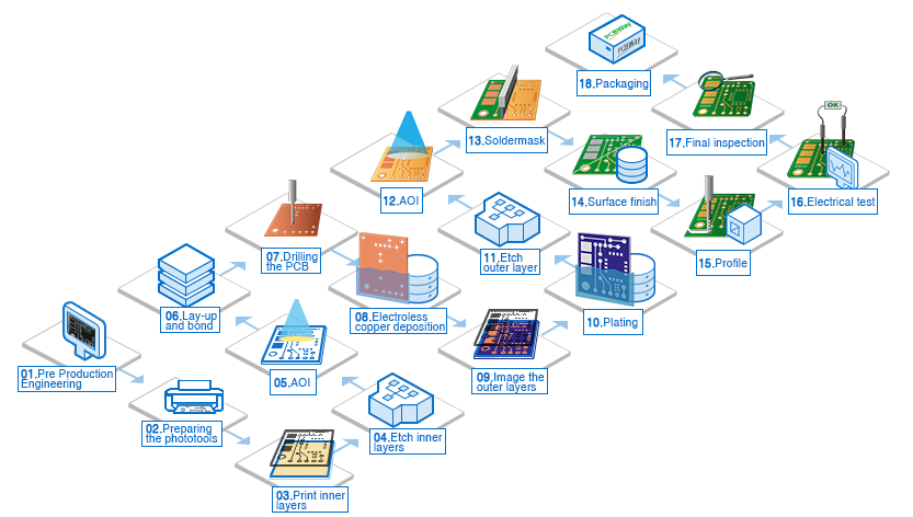
Making a PCB - PCB Manufacture step by step
Our Customers
 Military and aerospace: We have large customer base in these industries. Customers choose us to make their PCBs in the prototype and production stage.
 Medicine: Medicine and biomedical clients occupy a large part of our customers. We have strict quality standard and short lead time and our price is competitive, our customer base in this area is still on the rise.
 Commercial,
industrial and automotive: Most of our customers are in these industries. Fast response, short delivery time, professional engineering support continuously affordable price help retain and expand customer scale in these industries.
Commercial,
industrial and automotive: Most of our customers are in these industries. Fast response, short delivery time, professional engineering support continuously affordable price help retain and expand customer scale in these industries.
 University,
school and amateur: Students are our future scientists, we support them! Students and amateurs are price sensitive customers, our price guarantees they will rely on us for their PCB needs in terms of price and quality! At the same time, our educational sponsorship program provides free PCBs to university students, please send us the details of your project or competition at sales@multitech-pcb.com.
University,
school and amateur: Students are our future scientists, we support them! Students and amateurs are price sensitive customers, our price guarantees they will rely on us for their PCB needs in terms of price and quality! At the same time, our educational sponsorship program provides free PCBs to university students, please send us the details of your project or competition at sales@multitech-pcb.com.